
Application Note:


Moorfield graphene soft-etching technology allows for the controlled removal of graphene and 2D materials, without cross-linking photoresists that can lead to residual contamination that affects device performance.
For this, the technology implements low power plasmas (< 10 W) with fine power control (down to 20 mW), allowing material removal without collateral damage. This application note demonstrates the use of soft-etching technology implemented via a Moorfield nanoETCH tool as part of the successful production of a graphene Hall bar device.

1. Graphene grown by the CVD method (darker contrast), using a Moorfield nanoCVD-8G, is transferred onto an Si/SiO2 substrate. A photoresist Hall bar pattern (yellow) is formed on top of the graphene.

2. The photoresist is removed leaving the protected graphene. Importantly, the graphene surface is clean without any photoresist residue.

3. A nanoETCH system is used to expose the sample to precision soft-etching conditions. The image shows the sample after graphene removal (no contrast across the Si/SiO2 surface).

4. Further photolithography is used to define contact pads and leads ready for sample analysis.
Device performance
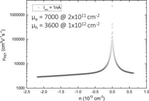
CVD graphene devices fabricated using the Moorfield nanoETCH have demonstrated high electron mobilities in excess of 7000 cm2/(Vs) at room temperature and negligible doping (see figure 1). In part, this is possible due to the soft-etching process employed that allows for the complete removal of unwanted graphene while leaving negligible residue on the top surface of remaining material that forms the functional part of the device.
Acknowledgements: All data supplied by Prof.Monica Craciun and Prof.Saverio Russo at the University of Exeter, UK.
Request more information