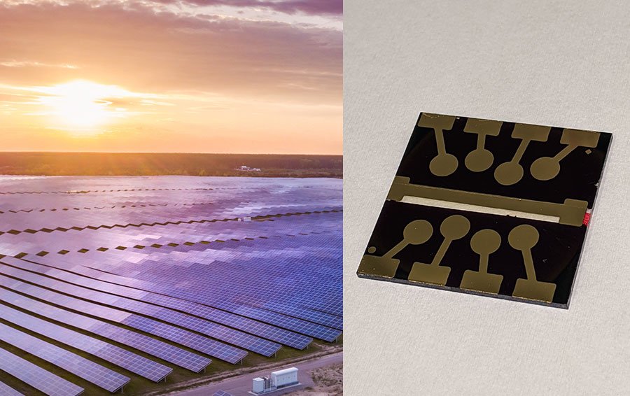
Much of the research conducted on next-generation solar cells is concerned with hybrid lead-halide perovskite materials. However, there has been a growing effort to find alternative compounds that offer similar or improved characteristics and remove the need for environmentally toxic lead, which thus far have been difficult to come by. It is important to find lead-free materials with a range of band gaps with the aim of combining them so that they generate electricity from complementary parts of the solar spectrum. Such a device is called a tandem solar cell, and will be a crucial tool in increasing the efficiency, and therefore decreasing the cost, of the future generations of solar cells.
Recently, PhD student Ben Putland supervised by Prof. Henry Snaith (Optoelectronic and Photovoltaic Device Group, University of Oxford) conducted cutting-edge research into the synthesis and photovoltaic performance of a novel inorganic lead-free halide solar absorber with the general formula A2BB’X6. Modelling suggests that, given the suitable bandgap of around 2 eV, this material could be used as a top cell absorber in tandem photovoltaic cells. In this case, modelling suggested it would pair well with the already well-established Si cells, to create a lead-free tandem cell with efficiencies exceeding 30%. Being entirely inorganic in composition, they may also offer a route to overcoming stability issues associated with existing organic-containing alternatives (e.g., hybrid perovskites) that often degrade rapidly under sustained exposure to sunlight.
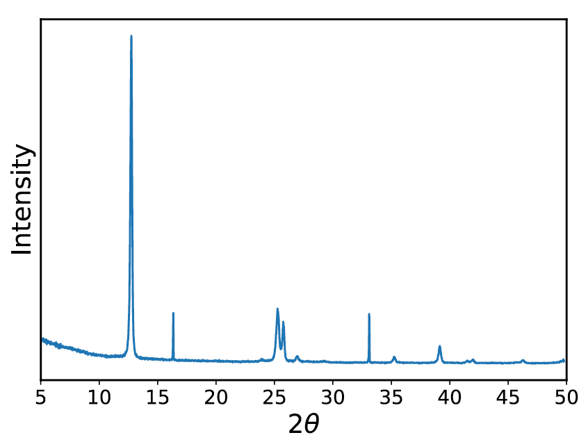
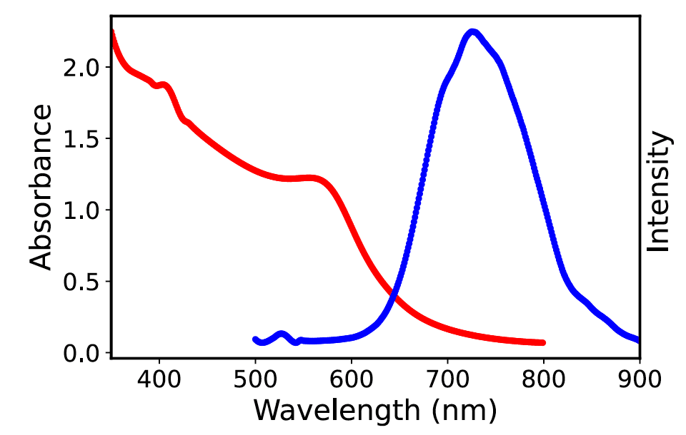
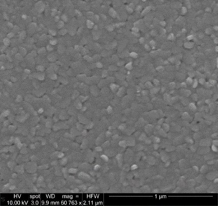
One issue with this novel material is its difficulty to process uniform films from solution. This is due to insolubility of the starting components and a complex crystallisation process which leads to undesirable dendritic crystal growth. Vacuum evaporation has allowed these problems to be overcome. With high levels of control, vacuum evaporation may offer the convenient and scalable ability for fabrication of these devices. The material was deposited through vacuum evaporation of three distinct precursors using equipment supplied by Moorfield. Characterisation of the material is shown below:
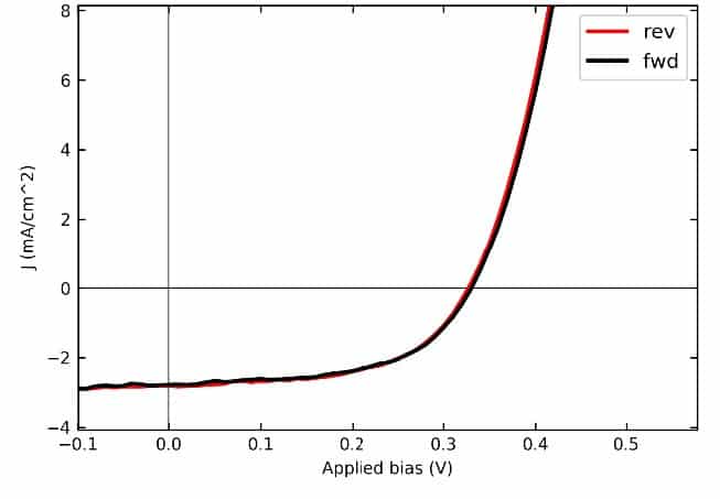
| Scan direction | Voc (V) | Jsc (mA cm-2) | FF (%) | PCE (%) |
| Forward | 0.35 | 2.80 | 54 | 0.53 |
| Reverse | 0.35 | 2.84 | 53 | 0.53 |
All data courtesy of the Optoelectronic and Photovoltaic Device Group, University of Oxford.
Although the power conversion efficiency is currently low at 0.53%, excitingly, these preliminary results show that the material can be formed by vacuum evaporation for photovoltaic applications. Work to refine the material properties as well as the device architectures is ongoing.
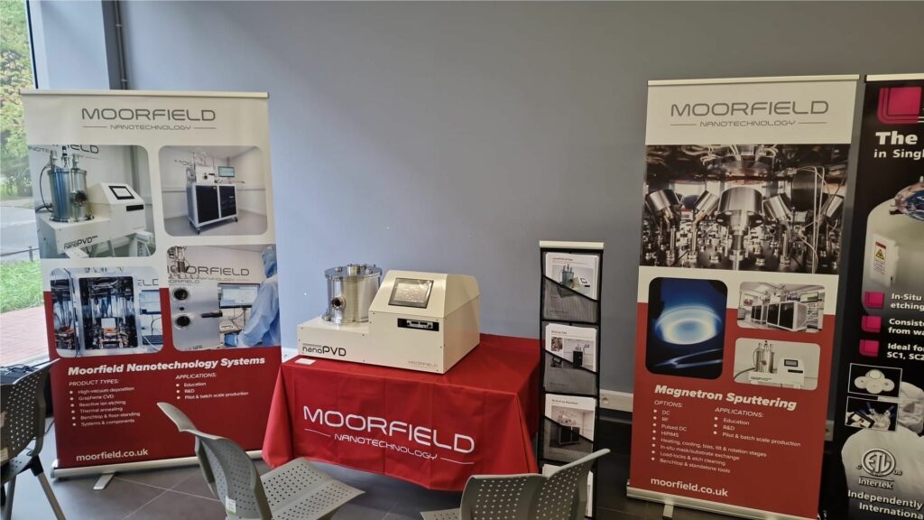
Moorfield LTE Sources and Systems
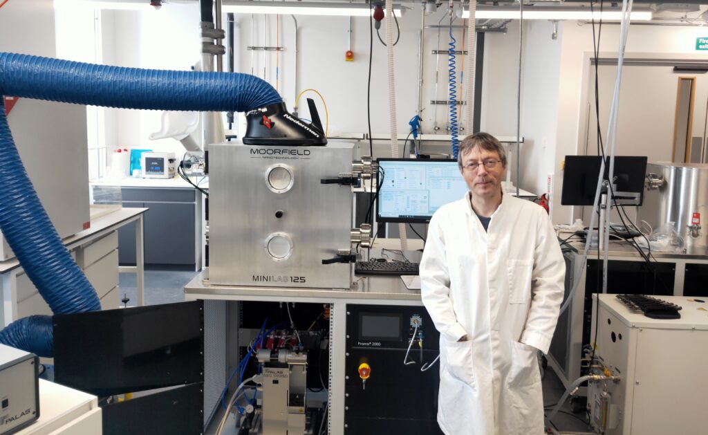
The researchers used a setup consisting of three Moorfield LTE cells and control units. The sources were operated in co-deposition mode (i.e., three sources running at once) and with precisely controlled individual deposition rates and thicknesses, measured with quartz crystal sensor heads, to allow for formation of material with the correct stoichiometry. Post-deposition annealing was then used to generate the required structure and properties.
With components optimised and field-proven for the highest levels of control when working with volatile evaporants, Moorfield LTE technology is now used worldwide for fabrication of devices ranging from OLEDs and organic FETs through to photovoltaics and perovskites. Hardware can be supplied as individual components for integration into an existing setup, or built into a fully integrated system based on the MiniLab or nanoPVD platforms.
Have a Project?
We are experts at matching deposition hardware to research requirements—call us today to discuss your current or future project.