A simple process for the fabrication of large-area CVD graphene based devices via selective in situ functionalization and patterning

Alexeev, A. A., et al. 2D Materials 2016 DOI: 10.1088/2053-1583/4/1/011010
This paper reports a simple method for the production of functional devices from CVD graphene (produced using a nanoCVD-8G system). Rather than forming devices on the application substrate after transfer, the authors demonstrate material patterning on the copper growth substrate, using lithography and plasma oxidation, pre-transfer. This simplifies growth-to-application pathways, and could allow use of a wider range of application substrates.

Link: http://iopscience.iop.org/article/10.1088/2053-1583/4/1/011010

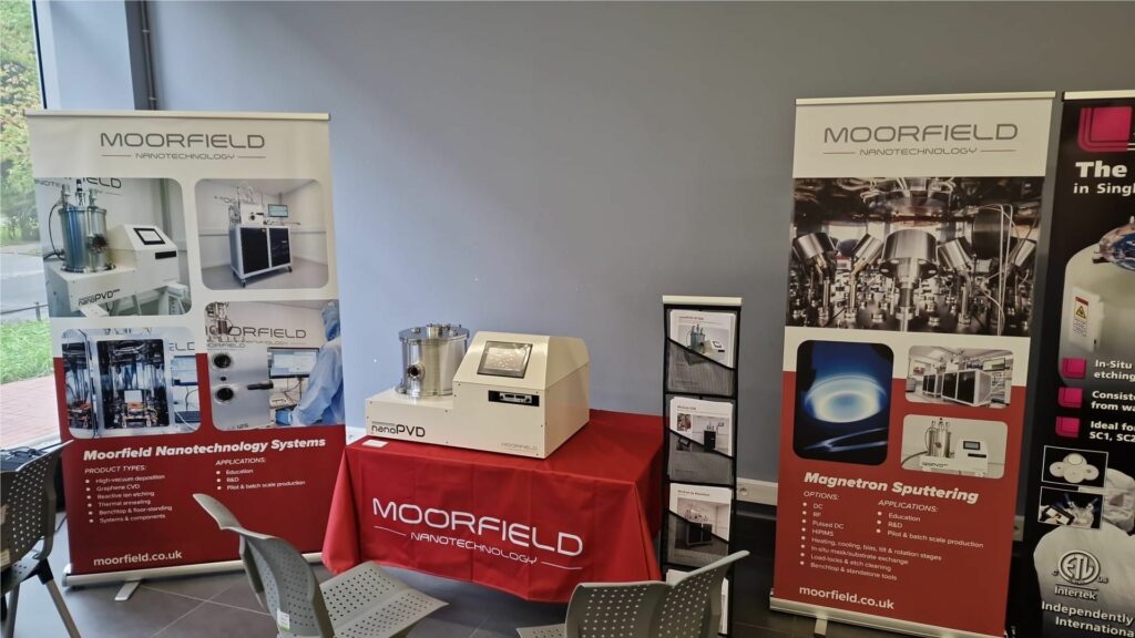
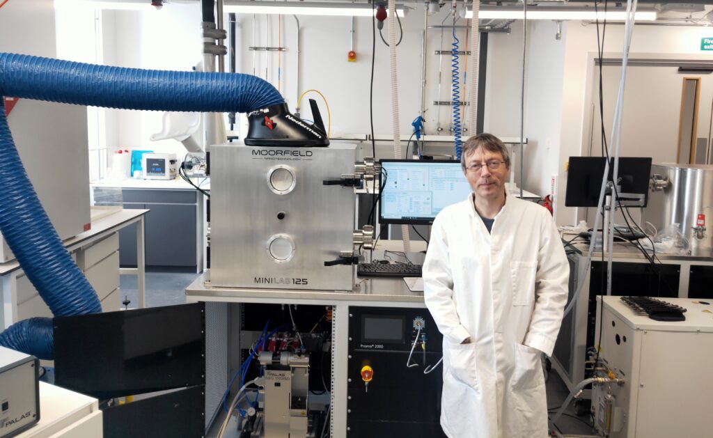
Moorfield products: nanoCVD-8G

Latest posts

MSE Supplies logo
MSE Supplies, Moorfield Announce Partnership for nanoPVD, nanoETCH, nanoCVD and ANNEAL Distribution in the United States.
Moorfield stand at Warsaw symposium
“Thin film engineering in photovoltaics, photonic structures and optoelectronics” symposium at the University of Warsaw.
DPG Logo
We’re at DPG exhibition at the University of Regensburg
We’re excited to confirm our presence at the DPG exhibition at the University of Regensburg, Germany, next month (6–9 September). We’ll be attending with Picovac — our agent for Germany and Austria….
Powder Aerosol Deposition Tools
University of Manchester take delivery of deposition tools…

Thank you for signing up