
During magnetron sputtering, a thin film is created on a substrate’s surface. Both film and substrate materials are dictated by the application and good adhesion between the two is critical. Unfortunately, good adhesion is not a given (delamination being the worst-case result), and careful consideration should be given to process and materials in order to optimise this.


This technical note provides an introductory explanation of adhesion and how this can be improved.
Film adhesion
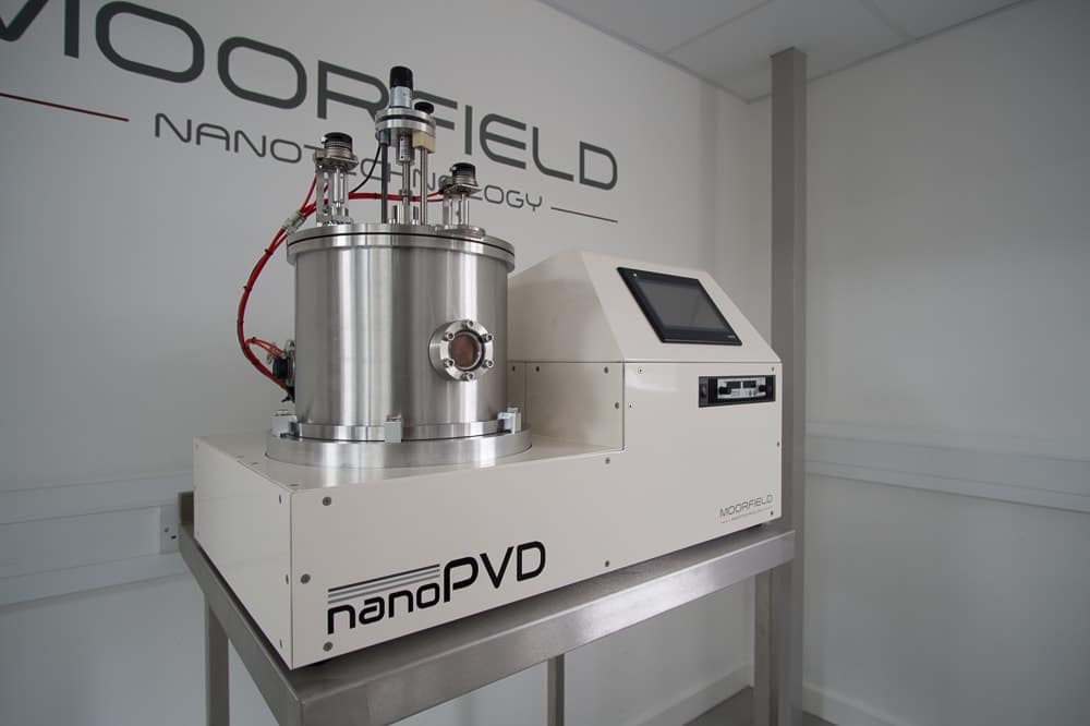
Figure 1: Moorfield desktop nanoPVD sputter system with a 90 mm throw distance as standard or variable position with substrate stage Z-shift.
Thermodynamically, adhesion can be defined as the work needed to overcome the interfacial energy between substrate and deposited material. The greatest component of this energy is chemical bonding. Mechanical locking and friction also contribute (usually to a lesser extent).
Adhesion energy, WA, can be defined as:
Here, γf, γs, and γfs are the surface energies of the film, substrate and film-substrate interface, respectively. Good adhesion is therefore promoted by maximising γfs and minimising γf and γs.
Surface cleaning
Surface dirt/impurities create local changes in energy, incurring preferential points for dislocations, shears or delamination. The same has been shown for residual moisture. As such, removal of contaminants through pre-process cleaning is a common way to improve adhesion.
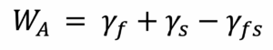
Surface dirt/impurities create local changes in energy, incurring preferential points for dislocations, shears or delamination. The same has been shown for residual moisture. As such, removal of contaminants through pre-process cleaning is a common way to improve adhesion. Solvent cleaning is one approach. For example, ultrasonication of samples in acetone and then isopropanol and drying with compressed gas is often effective. Other methods of cleaning can also be used. Pre-process annealing uses heat to drive off surface moisture, while plasma etching (see Figure 2) can be used to remove upper surface layers taking impurities with them.
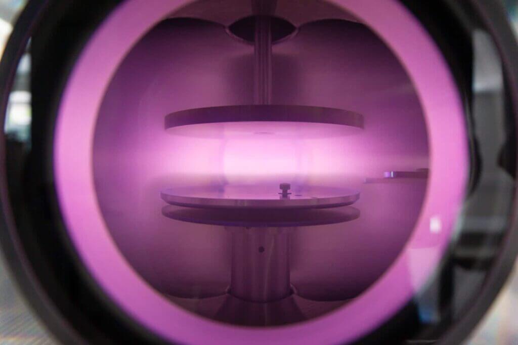
Figure 2: Moorfield 6” etch stage operating inside a load lock for pre-process substrate cleaning.
Process conditions
With sputtering underway, process conditions are highly influential. In adhesion, growth rate, sputtering power, substrate temperature and mean free path are particularly important:
Growth rate
Particles deposited on a substrate undergo surface diffusion. In time, this allows ad-atoms (deposited particles) to settle into minimum energy states providing better adhesion.
Figure 3: Moorfield 3” magnetron with adjustable angle and height being prepared in the demonstration laboratory.
Continued unchecked, this process would result in the theoretically lowest interfacial energy. However, further deposits terminate surface diffusion, thereby fixing their position. As such, slower deposition rates can increase adhesion by allowing more time for diffusion and settling. Rates can be controlled by sputtering power, process pressure, or altering the throw distance between source and substrate. Moorfield magnetrons, as seen in Figure 3, have adjustable height and angle for tight control of deposition geometry including throw distance.
Sputtering power
In general, particles arrive at substrates with energies similar to those with which they were released from the target. More energetic impacts with the target result in deposited particles having a higher average energy. Assuming all sputtering gas atoms are singularly ionised, the energy, E, of particles bombarding a targets surface is defined by:
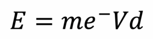
Here, m is the mass of a sputtering gas ion, e- is the charge of an electron, V is the field potential created by the voltage applied to the source, and d is the distance above the target surface at which a sputtering gas atom is ionised. Higher sputtering powers typically require higher applied voltages.
With sufficiently high energy, particles can arrive at the substrate and penetrate the surface in a process known as implantation. Implantation creates sites for bonding and encourages adhesion through the formation of intermediate layers. As such, high initial sputtering powers can be used to promote adhesion in some cases. While implantation may be advantageous, it should be noted that it can also change surface electrochemical properties due to the formation of a compositional gradient rather than a well-defined edge.
Substrate temperature
As above, particles arriving at substrates undergo random surface diffusion. Higher temperatures give ad-atoms more energy, allowing them to cover more distance in the same time, increasing their chance of finding low energy sites. As such, substrate temperature may also be used to improve adhesion. Temperature is best controlled with an in-chamber heating stage (can also be used for pre-process annealing). An example of a Moorfield silicon carbide 4” heating stage, capable of 800 °C substrate temperatures, can be seen in Figure 4.
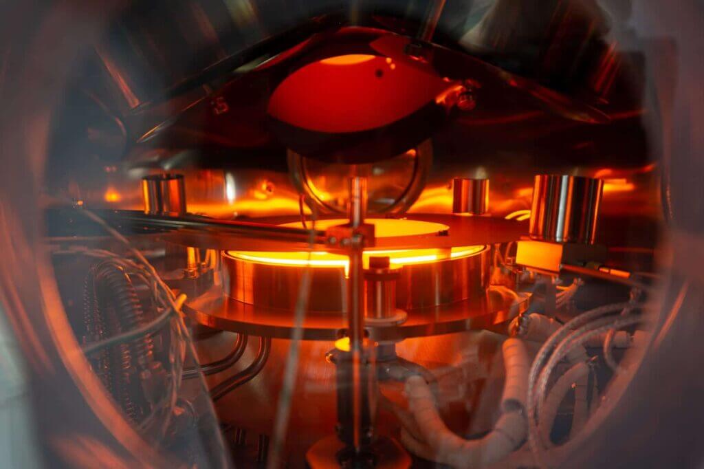
Figure 4: A Moorfield 4” 800 °C heating stage mounted in a MiniLab S125A system.
Mean free path
Governed by pressure, mean free path, λ, is given by:
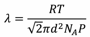
Here, R is the universal gas constant, T is temperature, d is the diameter of the relevant gas molecule, NA is Avogadro’s number and P is pressure. Effectively, λ dictates the number of collisions particles undergo as they move between source and substrate. If pressure is low enough , λ is approximately the throw distance (e.g., for argon gas at 8E-3 mbar, λ is 110 mm—typical sputtering throws are 80–150 mm)—there is then a good probability of particles arriving with the same energy thatas that they left the target with.
This may improve adhesion by promoting implantation or surface diffusion, as above. On the other hand, reducing λ (by increasing pressure) will reduce deposition rates; this may allow for greater levels of surface diffusion for the same applied sputtering power.
Buffer Layers
Control of sputtering conditions will allow for improved adhesion in many cases. However, in extreme cases it may be necessary to consider a buffer (or adhesion) layer to facilitate film growth. The choice of buffer layer will depend on the materials involved and sample requirements (i.e., effects on device properties). Examples include CdS can be used as a buffer on glass substrates for solar applications and ZnO mediates good growth of ITO.
Growth Mode
Interfacial stresses can cause lattice strain, which can lead to dislocations and film deformation. This becomes more pronounced for films of greater thickness, especially when entering the micron scale, or when attempting epitaxial growth.
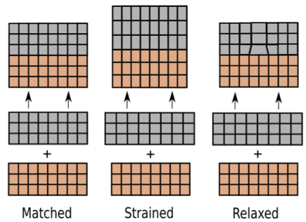
Figure 5: Left to right; matched, strained and relaxed lattice growth of a film, above in grey, on a substrate shown below in orange.
Poorly matched lattices will attempt to reduce strain in various ways, typically detrimental to sample quality, as shown in Figure 5. These can be avoided by choosing substrates with lattice parameters that closely match those of the deposited film (essential for epitaxy) or by using a buffer layer, as detailed above.
Substrate choice will also alter the way films grow. For example, metal films on insulating substrates are more likely to exhibit an island-like (Volmer-Weber) growth mode, as seen in Figure 6, due to ad-atoms bonding more strongly to each other than the substrate. Volmer-Weber growth is often desirable due to low lateral strain but a high density of grain boundaries may exist where islands meet. In contrast, step flow (Frank van der Merwe) growth, which results from lower inter-particle attractions, allows for greater surface diffusion. As above, this encourages particles into surface energy minima so that deposited films grow in a layer-by-layer manner.
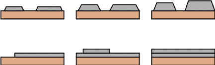
Figure 6: Volmer-Webber (island like growth) seen on top and Frank van der Merwe (step flow growth) seen below.
An example of this is the initial layers of Ag deposited on Pt. Such layer-by-layer growth supresses the formation of grain boundaries. However, if substrate-film lattice parameters are poorly matched lateral stresses can be high as the effects of mismatch propagate in the horizontal plane as the film grows.
Summary
This technical note details some key factors influencing substrate adhesion of sputtered films. Surface cleaning, control of process conditions, buffer layers and consideration of growth mode can all be used to optimise results. Moorfield specialise in the production of R&D and pilot-scale production magnetron sputtering systems and customise all designs per specific process requirements.
Request more information