

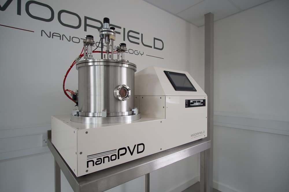
Wide-Area Benchtop PVD System
nanoPVD-S10A-WA Wide-Area PVD System
Compact wide-area RF/DC magnetron sputtering for larger research substrates and coating areas.
The nanoPVD-S10A-WA extends the compact nanoPVD sputtering workflow where standard 4 inch coverage is too restrictive, while keeping the system practical for research laboratories and cleanrooms.
 Powered by Bioz
Product gallery
nanoPVD-S10A-WA image carousel


Research-grade capability without enterprise complexity
This platform is positioned for research teams that need controllable thin-film process access, practical laboratory integration and clear configuration choices.
- Wide-area sputtering without moving straight to a large modular system
- RF/DC process flexibility for conductive and non-conductive materials
- Configurable source, gas and pressure-control options
- Recipe-led operation for repeatable research workflows
- Designed for research labs, cleanrooms and process development
Benefits that matter in a working research lab
Faster wide-area coating cycles
Bring larger-substrate PVD experiments closer to the research team and iterate coating geometry, recipe settings and film properties without waiting for larger shared tools.
Ease of use for mixed-experience teams
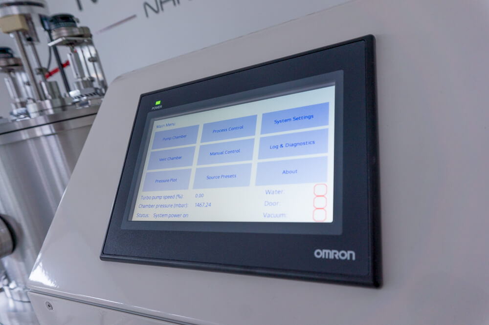
Touchscreen operation and recipe-led workflows support day-to-day use by researchers, students and technical teams working across changing projects.
Wide-area research flexibility
The platform extends compact nanoPVD workflows where standard benchtop coverage is too restrictive, while retaining configurable RF/DC sputtering options.
Lower operational friction
Add practical wide-area sputtering capability in a laboratory or cleanroom without the operational burden of production-scale equipment.
Better use of premium tools
Screen larger-area films locally, then move validated processes to central facilities only when throughput, wafer scale or advanced integration requires it.
Designed for device-relevant films
Useful for PV, sensors, optoelectronics, functional coatings, transparent conductive layers and larger-area materials-development samples.
Typical configurations
Use these examples as starting points. Moorfield can refine the final specification around your materials, substrates, gases, recipes and workflow constraints.
Wide-area metals deposition
For contact metals, electrodes and seed layers where coating area matters.
- RF/DC sputtering process
- Larger substrate coverage than standard compact systems
- Useful for device and coating R&D
TCO and dielectrics
For transparent conductive oxides and insulating films that need controlled sputter conditions.
- RF power option
- Oxygen process gas options
- Useful for PV, sensors and optoelectronics
Functional coatings
For exploratory coating workflows where compact footprint and larger coating area both matter.
- Research-friendly system scale
- Recipe-led process access
- Application-specific configuration
Not sure which configuration is right for your research?
Discuss Your ApplicationKey features
Compact laboratory footprint
Research-grade thin-film capability in a practical benchtop format.
Configurable process approaches
Build around sputtering, evaporation or hybrid workflows depending on the model.
Recipe-led control
Touchscreen HMI and recipe workflows improve day-to-day repeatability.
High-vacuum platform
Turbomolecular pumping supports clean, controlled deposition conditions.
Flexible gas and source options
Process gases, source count and monitoring options can be matched to the application.
Research-first support
Moorfield helps specify the platform around your materials and target films.
Options and upgrades
Configure the platform around the process approach, substrate handling, automation and laboratory services your application needs. Options are confirmed with quotation for the final build.
Technical specifications
Exact specifications depend on final configuration and should be confirmed with quotation.
| System type | Wide-area benchtop PVD / DC and RF magnetron sputtering |
|---|---|
| Base pressure | 5×10⁻⁷ mbar |
| Pressure control | Capacitance manometer + MFC closed-loop control as an option |
| Process gas inlets | Up to 3 MFC-controlled gases |
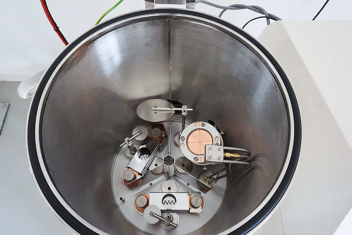
| Sputter sources | Up to 2 x 2″ water-cooled magnetrons |
| Target size | 2″ |
| Reactive sputtering | Yes; up to 3 MFCs with optional closed-loop control |
| Magnetic target sputtering | High-strength magnet pack available |
| Maximum substrate size | 8″ (200 mm) |
| Substrate heating | Up to 500°C optional |
| Substrate cooling | Available as an option |
| Substrate bias | RF and DC bias available as an option |
| Load lock | Not available as standard |
| Glovebox compatible | No |
| Process control | Industrial PLC + 7″ HMI touchscreen |
| Recipe control | Recipe save/load standard |
| Warranty | 2 years |
Applications
Application-library examples for wide-area and related nanoPVD sputtering workflows. The product cited is shown on each card so the evidence path stays clear.
MoO3 and Hard Carbon Architecture
Publication Title: Designing Molybdenum Trioxide and Hard Carbon Architecture for Stable Lithium-Ion Battery Anodes
Lead facility: Northumbria University
Moorfield product cited: nanoPVD-S10A-WA, nanoPVD-S10A
Read applicationInfluence of DC Sputtering Power on Ti Films
Publication Title: Influence of Sputtering DC Sputtering Power on the Surface Evolution of Ti Thin Films: A Fractal Description
Lead facility: University of Johannesburg
Moorfield product cited: nanoPVD-S10A
Read applicationHMR-Based Optical Gas Detection.
Publication Title: HMR-Based Optical Gas Detection With CuO and ZnO Coatings
Lead facility: Universidad Publica de Navarra
Moorfield product cited: nanoPVD-S10A
Read applicationEvolution of TiAlSi Thin Film Coatings
Publication Title: Evolution of TiAlSi thin film coatings under varying target power in DC magnetron sputtering
Lead facility: Northumbria University
Moorfield product cited: nanoPVD-S10A
Read applicationIn-situ monitoring of Aptamer-Protein binding
Publication Title: In Situ Monitoring of Aptamer–Protein Binding on a ZnO Surface Using Spectroscopic Ellipsometry
Lead facility: University of Liverpool
Moorfield product cited: nanoPVD-S10A
Read applicationsp2-rich dendrite-like carbon nanowalls
Publication Title: sp2 -rich dendrite-like carbon nanowalls as effective electrode for environmental monitoring of explosive nitroaromatic
Lead facility: Gdańsk University of Technology
Moorfield product cited: nanoPVD-S10A
Read applicationBioz citation lookup
Publication Title: Bioz citation results for nanoPVD-S10A-WA
Lead facility: Multiple published sources where available in Bioz
Moorfield product cited: nanoPVD-S10A-WA
View Bioz citationsResources and next steps
Related systems


Build the right nanoPVD-S10A-WA configuration for your research
Tell us about your materials, substrates, process gases and target films. Moorfield will help specify a practical system configuration.
nanoPVD-S10A-WA
Optimised for magnetron sputtering, the nanoPVD-S10A-WA is a Wide-Area configuration that extends the capabilities of the nanoPVD-S10A to allow for even coating of substrate diameters up to 8″, in a benchtop package.

nanoPVD-S10A-WA Benchtop PVD System
The wide-area version of the nanoPVD-S10A contains magnetron sputtering sources oriented directly upwards towards substrate platens. This arrangement in combination with substrate rotation and exposure plates with specially designed orifices allows for coating of substrates up to 8″ diameter for applications in which tight uniformity specifications are not critical.
Like the nanoPVD-S10A, magnetrons are water-cooled for sustained high-power operation and accept industry-standard targets. In addition, nanoPVD-S10A-WA units come with all attractive features of the nanoPVD range including turbomolecular pumping systems, recipe-based automated operation via touchscreen HMIs, and compact designs for benchtop location.
Key features
- Benchtop configuration
- Water-cooled magnetron sputtering sources for industry-standard 2″ targets
- MFC-controlled process gases
- DC and/or RF power supplies
- Fully automatic operation via touchscreen HMI
- Define/save multiple process recipes
- Up to 8” diameter substrates
- Base pressures <5 × 10⁻⁷ mbar
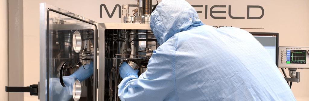
- Equipped for easy servicing
- Comprehensive safety features
- Cleanroom compatible
- Proven performance
Example Publications
Options
- Dry backing pump
- Fast chamber vent
- Automatic high-resolution pressure control
- Additional process gases
- 500 °C substrate heating stage
- Substrate rotation, Z-shift and shutters
- Up to 2 magnetron sputtering sources
- RF and/or DC power supplies
- SputterSwitch power supply/source switching technology
- Co-deposition
- Quartz crystal sensor head


Typical configurations
The nanoPVD-S10-WA is a semi-custom tool, with final design being subject to customer requirements.
Service requirements
All nanoPVD-S10A systems require chilled water, dry compressed air, nitrogen for venting (optional), process gas supplies, and electrical power. Exact requirements will be provided with quotations or on request.
Protect your investment and maximise uptime
 Your Moorfield system is a long-term asset that needs to operate reliably and repeatably. A Service Plan is designed to protect your investment by reducing unplanned downtime, improving system reliability, and giving your team faster access to expert support when you need it.
All plans include an annual preventive maintenance visit (with documented checks) plus remote technical support—helpful for troubleshooting issues quickly without waiting for an on-site visit. As your needs increase, higher tiers add greater consumables/parts cover, discounted call-outs and travel, priority scheduling, and training refresher days to help new users get up to speed and reduce avoidable errors.
Service Plans also support easier budgeting (fixed annual or monthly options on eligible tiers) and provide multi-system discounts.
Ask us which plan best fits your throughput demands and budget priorities using our CONTACT US FORM