

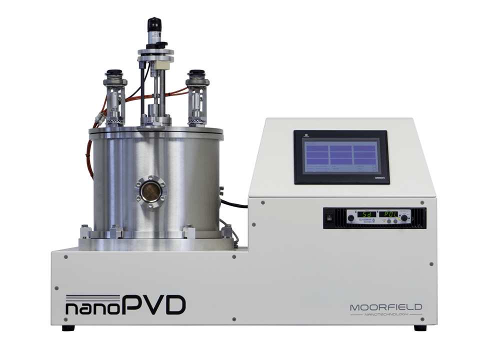
Benchtop PVD System
nanoPVD-S10A Benchtop PVD System
Compact, research-grade RF/DC magnetron sputtering for advanced thin-film materials.
The nanoPVD-S10A brings high-performance sputtering capability into a compact benchtop platform, supporting metals, oxides, nitrides, multilayers, and exploratory materials R&D.
 Powered by Bioz
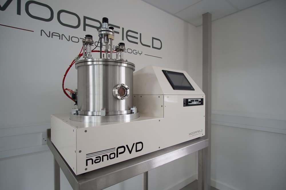
Product gallery
nanoPVD-S10A image carousel


Research-grade sputtering in a compact benchtop platform
The nanoPVD-S10A is compact enough for research laboratories and cleanrooms, while using high-end vacuum, source and control hardware for controlled thin-film deposition. It is optimised for RF and DC magnetron sputtering of metals and insulating materials, giving research teams a practical platform for repeatable materials development.
- Compact footprint for research labs and cleanrooms
- RF/DC compatibility for a broad material range
- Configurable sources and gas handling
- Recipe-driven operation via touchscreen HMI
- Designed for serviceability and long-term use
Benefits that matter in a working research lab
Faster experimental cycles
Keep early-stage sputtering work close to the research group, reduce waiting time and make process changes without competing for flagship cleanroom capacity.
Ease of use for mixed-experience teams
A touchscreen HMI, compact layout and straightforward maintenance help new users build confidence while still working on genuine research-grade sputtering processes.
Research-grade flexibility
RF and DC sputtering capability supports metals and insulating materials, including reactive and co-deposition methods for more advanced film stacks.
Lower operational friction
The benchtop format helps departments add local PVD capability without creating the access, facility and training burden associated with larger infrastructure.
Better use of premium tools
Develop and screen baseline recipes locally, then transfer mature work to larger shared systems only when the process is ready.
Designed for real devices
Useful for contact layers, seed films, functional coatings, TCO/dielectric studies, reactive sputtering and multi-material research workflows.
Key features for thin-film process development
Designed for laboratories that need repeatable sputtering capability without production-scale complexity.
Compact benchtop design
Advanced PVD capability in a space-efficient format for research labs, teaching spaces and cleanrooms.
RF/DC magnetron sputtering
DC sputtering for conductive materials and RF sputtering for conductive and non-conductive materials such as oxides and nitrides.
High-vacuum performance
Turbomolecular pumping supports low-contamination operation with base pressure below 5E-07 mbar.
Reactive sputtering capability
Gas and pressure control can support up to three process gases for oxide, nitride and compound film development.
Recipe-based touchscreen control
Touchscreen HMI with fully automatic operation and the ability to define and save multiple process recipes.
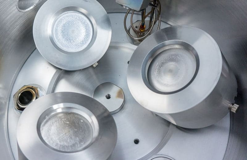
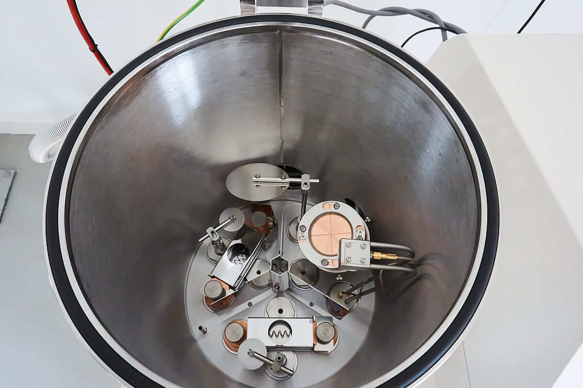
Configurable source and gas options
Up to three water-cooled magnetron sources for industry-standard 2" targets, with co-deposition and reactive process options.
Typical nanoPVD-S10A configurations
Start with a proven configuration, then tailor source, gas, stage and monitoring options around your materials and target films.
Metals deposition
For conductive films, contact metals, electrodes and exploratory materials work where reliable DC sputtering and practical geometry control matter.
- Two magnetrons with DC power supply
- SputterSwitch module for shared output
- Substrate Z-shift and bi-shutter for best 4" substrate geometries
- Quartz crystal sensor head for rate and thickness calibration
TCO / dielectrics sputtering
For transparent conductive oxides, dielectric coatings and process approaches that benefit from RF power and oxygen control.
- Two magnetrons with RF power supply
- SputterSwitch module for shared output
- Substrate heating and additional oxygen process gas line
- Substrate Z-shift, bi-shutter and quartz crystal sensor head
Reactive / co-deposition
For flexible materials R&D where researchers need source routing, multiple gases and mixed RF/DC process capability.
- Three magnetrons with RF and DC power supplies
- SputterSwitch for flexible power supply/source routing
- Three process gases, for example argon, oxygen and nitrogen
- Reactive deposition of oxides and nitrides
Not sure which configuration you need?
Discuss Your ApplicationOptions and upgrades
Configure the platform around the process approach, substrate handling, automation and laboratory services your application needs. Options are confirmed with quotation for the final build.
Vacuum and gas handling
- Dry backing pump
- Fast chamber vent
- Capacitance manometer and optional MFC closed-loop pressure control
- Up to 3 MFC-controlled process gases
Deposition and power
- Up to 3 x 2" water-cooled magnetron sputtering sources
- 780 W DC and/or 150 W, 13.56 MHz RF power supplies with auto-match
- High-strength magnet pack for magnetic target sputtering
- SputterSwitch source/power routing where specified
- In-situ rate and thickness monitoring
Substrate handling
- Substrate heating up to 500°C; up to 600°C with 4-bulb configuration
- Substrate cooling option
- RF and DC substrate bias option
- Rotation, Z-shift and shutters where specified
Technical specifications
Exact specifications depend on final configuration and should be confirmed with quotation.
| System type | Benchtop PVD / DC and RF magnetron sputtering |
|---|---|
| Base pressure | 5×10⁻⁷ mbar |
| Pressure control | Capacitance manometer + MFC closed-loop control as an option |
| Process gas inlets | Up to 3 MFC-controlled gases |
| Sputter sources | Up to 3 x 2" water-cooled magnetrons |
| Target size | 2" |
| Reactive sputtering | Yes; up to 3 MFCs with optional closed-loop control |
| Magnetic target sputtering | High-strength magnet pack available |
| Maximum substrate size | 4" (100 mm) |
| Substrate heating | Up to 500°C optional; up to 600°C with 4-bulb configuration |
| Substrate cooling | Available as an option |
| Substrate bias | RF and DC bias available as an option |
| Load lock | Not available as standard |
| Glovebox compatible | No |
| Process control | Industrial PLC + 7" HMI touchscreen |
| Recipe control | Recipe save/load standard |
| Footprint | 800 x 500 x 550 mm |
| Warranty | 2 years |
Applications
Application-library examples and Bioz lookup results showing nanoPVD-S10A sputtering used in published thin-film, sensor, coating, graphene and device-R&D work.
Influence of DC Sputtering Power on Ti Films
Publication Title: Influence of Sputtering DC Sputtering Power on the Surface Evolution of Ti Thin Films: A Fractal Description
Lead facility: University of Johannesburg
Moorfield product cited: nanoPVD-S10A
Read applicationHMR-Based Optical Gas Detection.
Publication Title: HMR-Based Optical Gas Detection With CuO and ZnO Coatings
Lead facility: Universidad Publica de Navarra
Moorfield product cited: nanoPVD-S10A
Read applicationEvolution of TiAlSi Thin Film Coatings
Publication Title: Evolution of TiAlSi thin film coatings under varying target power in DC magnetron sputtering
Lead facility: Northumbria University
Moorfield product cited: nanoPVD-S10A
Read applicationDirect synthesis of nanopatterned graphene
Publication Title: Direct synthesis of nanopatterned epitaxial graphene on silicon carbide
Lead facility: University of Technology Sydney
Moorfield product cited: nanoPVD-S10A
Read applicationIn-situ monitoring of Aptamer-Protein binding
Publication Title: In Situ Monitoring of Aptamer–Protein Binding on a ZnO Surface Using Spectroscopic Ellipsometry
Lead facility: University of Liverpool
Moorfield product cited: nanoPVD-S10A
Read applicationBiocompatible beta-Ti3Au intermetallic film surfaces
Publication Title: Adatom controlled emergence of high hardness in biocompatible beta-Ti3Au intermetallic thin film surfaces
Lead facility: Northumbria University
Moorfield product cited: nanoPVD-S10A
Read applicationBioz citation lookup
Publication Title: Bioz citation results for nanoPVD-S10A
Lead facility: Multiple published sources where available in Bioz
Moorfield product cited: nanoPVD-S10A
View Bioz citationsBuilt for day-to-day usability
The nanoPVD-S10A is designed to make advanced sputtering practical for busy research environments: quick to learn, straightforward to service and flexible enough to remain useful as research priorities evolve.
- Comprehensive safety features
- Touchscreen operation
- Recipe storage
- Easy servicing
- Low running costs
- Cleanroom compatible
Resources and next steps
Review the product PDF, contact Moorfield for configuration guidance, or compare related nanoPVD platforms.
Product PDF
Download the nanoPVD-S10A brochure for a concise platform overview.
Download Product PDFContact an expert
Share your materials, substrates, process gases and target films with the Moorfield team.
Contact UsRequest a quote
Move from configuration discussion to a formal quotation for your lab.
Request a QuoteRelated systems


Product FAQ
Frequently asked questions
What is the maximum substrate size for the nanoPVD-S10A?
The nanoPVD-S10A supports substrates up to 4 inches (100 mm) in diameter as standard.
Can the nanoPVD-S10A sputter insulating materials?
Yes. The system supports RF sputtering for non-conductive materials including oxides and nitrides, alongside DC sputtering for conductive targets.
Is the nanoPVD-S10A compatible with glovebox transfer?
No. The nanoPVD-S10A is not listed as glovebox compatible. For protected-transfer or air-sensitive workflows, contact Moorfield to discuss MiniLab glovebox-compatible configurations.
What base pressure does the nanoPVD-S10A achieve?
The system achieves a base pressure below 5E-07 mbar using turbomolecular pumping.
Can multiple users run different recipes on the nanoPVD-S10A?
Yes. The touchscreen HMI supports recipe save and load, allowing multiple users and projects to store and recall their own deposition parameters.
Build the right nanoPVD-S10A configuration for your research
Tell us about your materials, substrates, process gases, and target films. Moorfield will help specify the right configuration.