

Home > Technique resource > Thin-film deposition overview
Foundation guide
Thin-film deposition overview
Thin-film deposition changes the surface or structure of a substrate by adding controlled layers of material. This guide helps researchers distinguish between PVD, CVD, plasma and thermal-process steps, then move toward a suitable Moorfield platform discussion.
Plain language guide
What this means in practice
Thin-film deposition is the umbrella term for putting a controlled layer of material onto a substrate. For a new researcher, the first split is usually between adding material by vacuum deposition, changing a surface with plasma, or changing a film after deposition with heat treatment.
What happens in the system
- Define the target film: metal, oxide, nitride, organic, nanoparticle, graphene or another functional material.
- Match the material to a process family: sputtering, evaporation, CVD, plasma etch or anneal.
- Check the practical constraints: substrate size, temperature sensitivity, atmosphere, contamination risk, throughput and whether the work must stay close to the research group.
What changes the result
- The same material can behave differently depending on source geometry, pressure, substrate temperature and surface preparation.
- Early recipe work often benefits from local access because small changes to pre-clean, rate, gas flow or thermal step can change the result.
- A good specification starts with the material and film target, not with a product name.
Questions to answer first
- Are you adding material, removing material, cleaning a surface or thermally treating a film?
- Is the substrate sensitive to plasma, temperature, oxygen or moisture?
- Do you need a compact benchtop tool, a modular platform, protected transfer or a shared-facility complement?
Further reading
Useful external explainers
These neutral references are included to help newer readers understand the underlying process family. Moorfield system suitability still depends on a configuration discussion.
When it helps
Where this technique fits in research workflows
A practical overview of thin-film deposition methods used in advanced materials, device and coatings research. Moorfield can help connect the process requirement to a practical benchtop or modular configuration without treating the guide as a final specification.
When the process is not fixed yet
Use the overview to compare sputtering, evaporation, CVD, etch and anneal as separate process choices before specifying a tool.
When a shared facility is limiting iteration
Identify which process steps could be moved closer to the research group for faster local recipe development.
When multiple techniques may be needed
Explore whether a benchtop or modular platform is more appropriate for the material set and workflow.
Configuration thinking
Map the process need to a platform discussion
The table below is guidance for early selection conversations. It deliberately avoids over-specifying performance before Moorfield has reviewed the material set and lab environment.
| Research need | Relevant process consideration | Potential Moorfield fit |
|---|---|---|
| Need to deposit conductive films | Start with PVD and sputtering/evaporation choices | nanoPVD or MiniLab discussion |
| Need to deposit sensitive organic or volatile materials | Consider thermal or low-temperature evaporation where material behaviour allows | nanoPVD-T15A or modular evaporation discussion |
| Need to clean, activate or etch surfaces | Separate plasma etch requirements from deposition requirements | nanoETCH or MiniLab plasma process discussion |
| Need controlled thermal processing | Define temperature, atmosphere and sample handling first | nanoANNEAL discussion |
Relevant platforms
Systems to consider
Start with the process requirement, then compare platform size, source options, atmosphere control, substrate handling and future expansion needs.
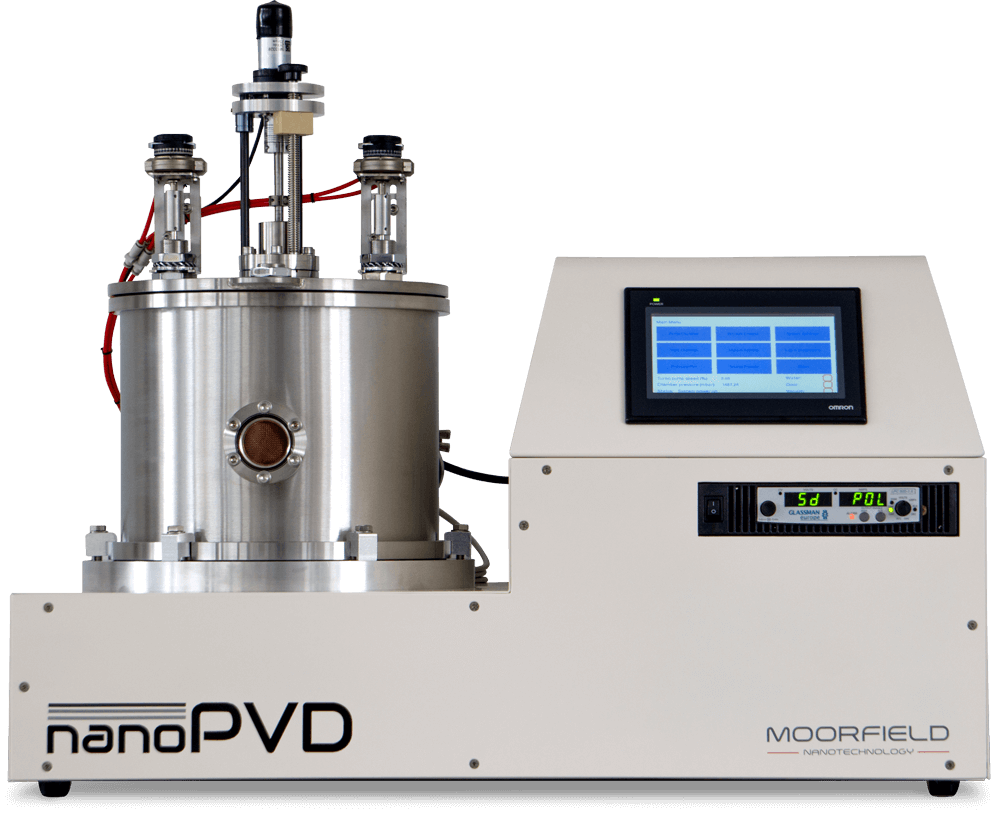
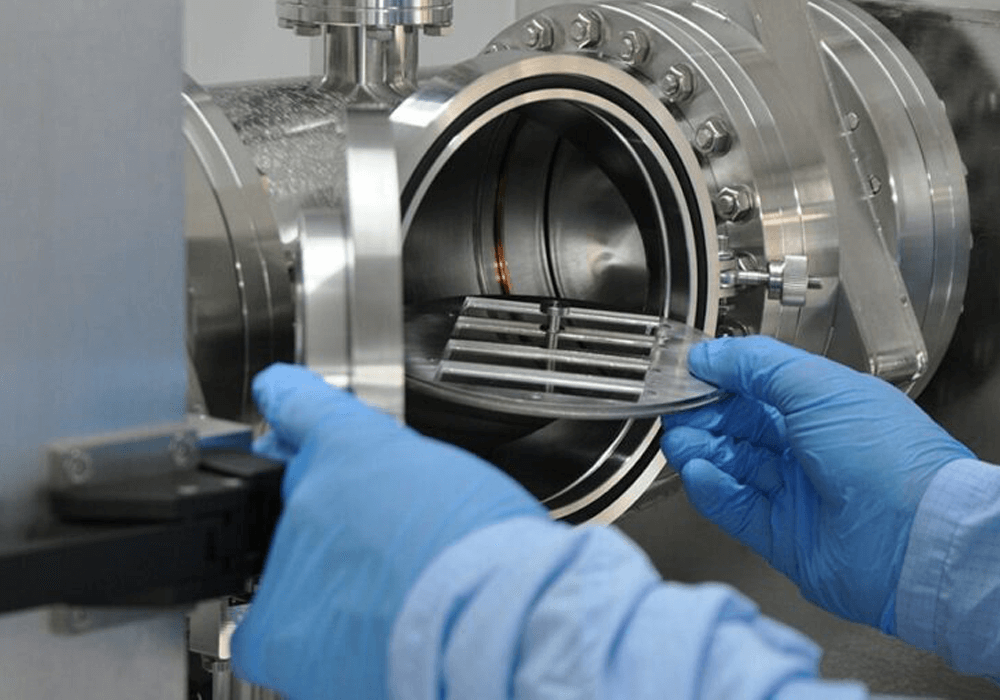
nanoPVD benchtop systems
Compact deposition systems for local sputtering, evaporation and combined thin-film process development.
Explore
MiniLab modular PVD
Configurable modular platforms for more complex source, chamber, transfer and sample-handling requirements.
Explore
Material selector
Look up chart-based deposition guidance by material before starting a configuration discussion.
ExploreContinue learning
Related technique guides
Move between technique pages to compare process families before using the selector or contacting Moorfield.
Next step
Need help choosing a process?
Tell Moorfield about your material set, substrate size, source preference and target film stack. We can help identify a practical platform and configuration.
Thin Film Deposition System: Precision Technology for Advanced Coatings
A thin film deposition system is a high-precision tool used to deposit ultra-thin layers of material onto a surface, or substrate. These systems enable the creation of custom coatings with unique optical, electrical, and mechanical properties. Widely used in industries like semiconductors, optics, and renewable energy, thin film deposition systems are essential for advancing modern technology.
How Does Thin Film Deposition Work?
Thin film deposition systems work by depositing a controlled amount of material onto a surface. Depending on the technique, this may be achieved through either Physical Vapor Deposition (PVD) or Chemical Vapor Deposition (CVD). Each approach offers specific benefits and is chosen based on the application requirements.
Physical Vapor Deposition (PVD)
PVD involves transforming solid material into vapor, which then condenses onto the substrate. Key PVD methods include:
Magnetron Sputtering Deposition: Atoms are ejected from a target material using a high-energy ion bombardment, which then deposit onto the substrate.
Thermal Evaporation: Material is heated until it vaporizes, allowing it to recondense on the substrate.
Electron Beam Evaporation (e-beam evaporation): Uses an electron beam to heat and vaporize the source material for deposition.
Chemical Vapor Deposition (CVD)
CVD relies on chemical reactions to produce a thin film on the substrate. Common techniques include:
Atmospheric Pressure CVD (APCVD): Deposition at standard atmospheric pressure, suitable for large-scale production.
Low Pressure CVD (LPCVD): Operates at reduced pressure to produce higher-quality films.
Plasma-Enhanced CVD (PECVD): Uses plasma to lower reaction temperatures, ideal for temperature-sensitive substrates.
—
Applications
Thin film deposition is critical to the production of high-performance materials used in a variety of industries.
Semiconductors & Electronics
– Creation of integrated circuits (ICs), transistors, and microchips.
– Enables miniaturization of electronic components for consumer devices like smartphones and laptops.
Optics & Photonics
– Anti-reflective coatings for lenses, displays, and optical sensors.
– Reflective coatings for mirrors and laser optics.
Renewable Energy
– Production of thin-film solar cells (CdTe, CIGS) to enhance efficiency and lower production costs.
Medical Devices
– Biocompatible coatings for stents, implants, and surgical tools.
– Improved wear resistance and friction reduction for medical devices.
Industrial Coatings
– Protective coatings for cutting tools and industrial machinery to extend lifespan.
– Wear-resistant coatings for automotive and aerospace components.
Choosing the Right Thin Film Deposition System
With a range of deposition techniques available, selecting the right system is crucial for achieving performance and production goals. Key factors to consider include:
Deposition Technique: PVD is ideal for wear-resistant coatings, while CVD is best for large-scale semiconductor production.
Material Requirements: Different materials (metals, oxides, nitrides) may favor certain deposition methods.
Substrate Compatibility: Ensure the system can handle the size, shape, and material of your substrates.
Temperature Needs: Some substrates require low-temperature deposition, necessitating PECVD or similar systems.
Production Volume: High-throughput production may require batch or inline processing capabilities.
A thin film deposition system is a critical tool for industries requiring precise, high-performance coatings. From semiconductor manufacturing to medical devices, the ability to deposit thin films with atomic-level precision enables companies to innovate and stay ahead of the competition. Whether you’re involved in R&D or large-scale production, selecting the right system is key to achieving superior product performance and operational efficiency.
If you want to learn more about the PVD and CVD systems we offer, please browse our products or contact us to discuss your requirements.
