

Home > Technique resource > Magnetron sputtering
PVD technique
Magnetron sputtering
Magnetron sputtering uses a plasma to eject atoms from a target material so they can deposit as a thin film on a substrate. DC sputtering is commonly used for conductive targets, while RF sputtering can support insulating materials such as oxides and nitrides by configuration.

Plain language guide
What this means in practice
Magnetron sputtering uses a plasma to knock atoms out of a solid target. Those atoms then land on the substrate and form a thin film. Researchers often choose sputtering when they need robust metal, oxide, nitride or multilayer film development.
What happens in the system
- A process gas, normally argon for basic sputtering, is introduced into a low-pressure chamber.
- Electrical power creates a plasma near the target; ions from the plasma hit the target surface.
- Target atoms are ejected and deposit on the substrate; reactive gases can be added for oxide or nitride films where the system is configured for it.
What changes the result
- DC sputtering is normally used with conductive targets; RF sputtering is used when insulating targets are part of the material set.
- Pressure, power, target-substrate distance and gas chemistry can all change film density, stress, rate and composition.
- Reactive sputtering requires careful gas and pressure control because the target surface and growing film can change during the run.
Questions to answer first
- Are your targets conductive, insulating or a mixture of both?
- Do you need single-layer films, multilayers, reactive films or co-deposition?
- How much substrate coverage and uniformity do you need at this stage of the research?
Further reading
Useful external explainers
These neutral references are included to help newer readers understand the underlying process family. Moorfield system suitability still depends on a configuration discussion.
When it helps
Where this technique fits in research workflows
Plasma-based thin-film deposition from a target material, used for metals, compounds and reactive film development by configuration. Moorfield can help connect the process requirement to a practical benchtop or modular configuration without treating the guide as a final specification.
Conductive layers and contacts
Consider sputtering for metals, conductive films, adhesion layers and device-relevant contact stacks.
Oxides, nitrides and compounds
RF and reactive sputtering configurations can support insulating or compound material studies where appropriate.
Multilayers and co-deposition
Multiple sources and source switching can support exploratory multilayer or composition-development work.
Configuration thinking
Map the process need to a platform discussion
The table below is guidance for early selection conversations. It deliberately avoids over-specifying performance before Moorfield has reviewed the material set and lab environment.
| Research need | Relevant process consideration | Potential Moorfield fit |
|---|---|---|
| Metal contact or electrode films | DC magnetron sputtering | nanoPVD-S10A or MiniLab |
| Oxide or nitride films | RF or reactive sputtering by configuration | nanoPVD-S10A, nanoPVD-ST15A or MiniLab |
| Multi-material film stacks | Multiple sources and shutters/source switching | nanoPVD-ST or MiniLab platform discussion |
| Small-batch research access | Compact sputtering capability near the research group | nanoPVD range |
Relevant platforms
Systems to consider
Start with the process requirement, then compare platform size, source options, atmosphere control, substrate handling and future expansion needs.
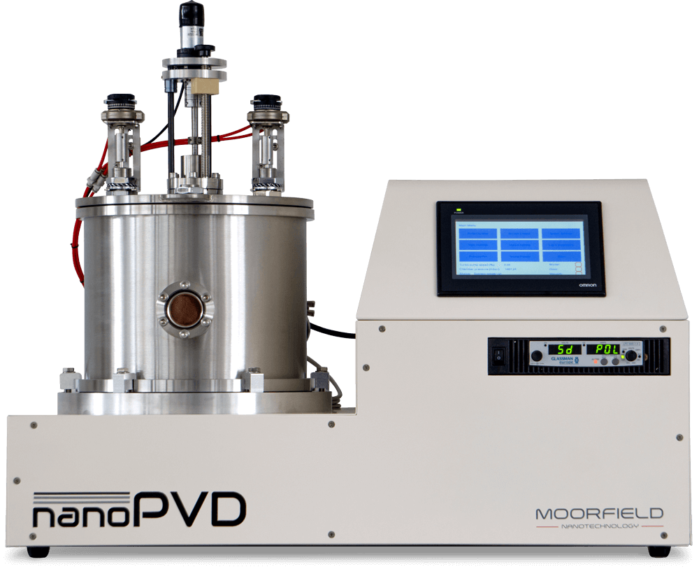
nanoPVD benchtop systems
Compact deposition systems for local sputtering, evaporation and combined thin-film process development.
Explore
MiniLab modular PVD
Configurable modular platforms for more complex source, chamber, transfer and sample-handling requirements.
Explore
Material selector
Look up chart-based deposition guidance by material before starting a configuration discussion.
ExploreContinue learning
Related technique guides
Move between technique pages to compare process families before using the selector or contacting Moorfield.
Next step
Need help choosing a process?
Tell Moorfield about your material set, substrate size, source preference and target film stack. We can help identify a practical platform and configuration.
Magnetron sputtering: the basics of how it works
In magnetron sputtering, magnetic fields focus plasmas onto target material surfaces, ejecting material that moves through the plasma to coat substrates. Suitable for depositing most materials (with correct choice of sputtering power supply).
Physical Vapour Deposition (PVD) is a widely used technique for depositing thin films and coatings. A magnetron source is a critical component in this process, providing a means to efficiently sputter material from a target onto a substrate. The magnetron enhances the sputtering process by using a magnetic field to confine electrons close to the target surface, increasing the ionisation efficiency and sputter rate.
How The Magnetron Source Works
Magnetron sputtering involves bombarding a target material with high-energy ions (typically Argon ions). The collision dislodges atoms from the target, which then deposit onto the substrate. The magnetron source utilizes a magnetic field, created by magnets behind the target, to trap electrons near the target surface. Electrons, influenced by the magnetic field, follow helical paths, increasing their chance of ionizing the gas. The positively charged Argon ions are attracted to the negatively charged target, causing sputtering.
The sputtered atoms travel through the vacuum and deposit as a thin film on the substrate.
Choice of DC vs. RF Power Supply
DC Power Supply:
Used for sputtering conductive materials such as metals. A direct current (DC) power supply provides a constant voltage and current, creating a stable plasma.
- Advantages: Simplicity, cost-effectiveness, and efficiency for conducting targets.
- Limitations: Not suitable for insulating or dielectric materials, as the constant current can lead to charge buildup and arcing on the target surface.
RF Power Supply:
Used for sputtering both conductive and non-conductive materials. Radio frequency (RF) power supplies operate at high frequencies (typically 13.56 MHz), alternating the current rapidly to prevent charge buildup.
- Advantages: Versatility in sputtering a wide range of materials, including insulators and dielectrics. The alternating current prevents arcing and allows for uniform sputtering.
- Limitations: More complex and expensive than DC power supplies, with potentially lower sputter rates for conductive materials compared to DC.
Target Considerations
- Choice of Material: Depends on the desired coating. Common materials include metals (e.g., aluminium, titanium), alloys, and compounds.
- Target Thickness: Should be sufficient to avoid frequent replacements, but not too thick to cause issues with heat dissipation.
- Some thin or brittle targets may need a backing to provide support and prevent accidental cracking during use.
Substrate Preparation
- Cleanliness: Substrates must be clean and free from contaminants to ensure good adhesion and uniformity.
- Some PVD systems offer a substrate pre-clean using an in-chamber or load lock etch station.
- Temperature: Some processes require heating of the substrate to improve film quality and adhesion.
