

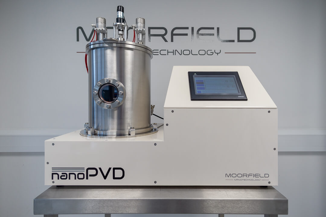
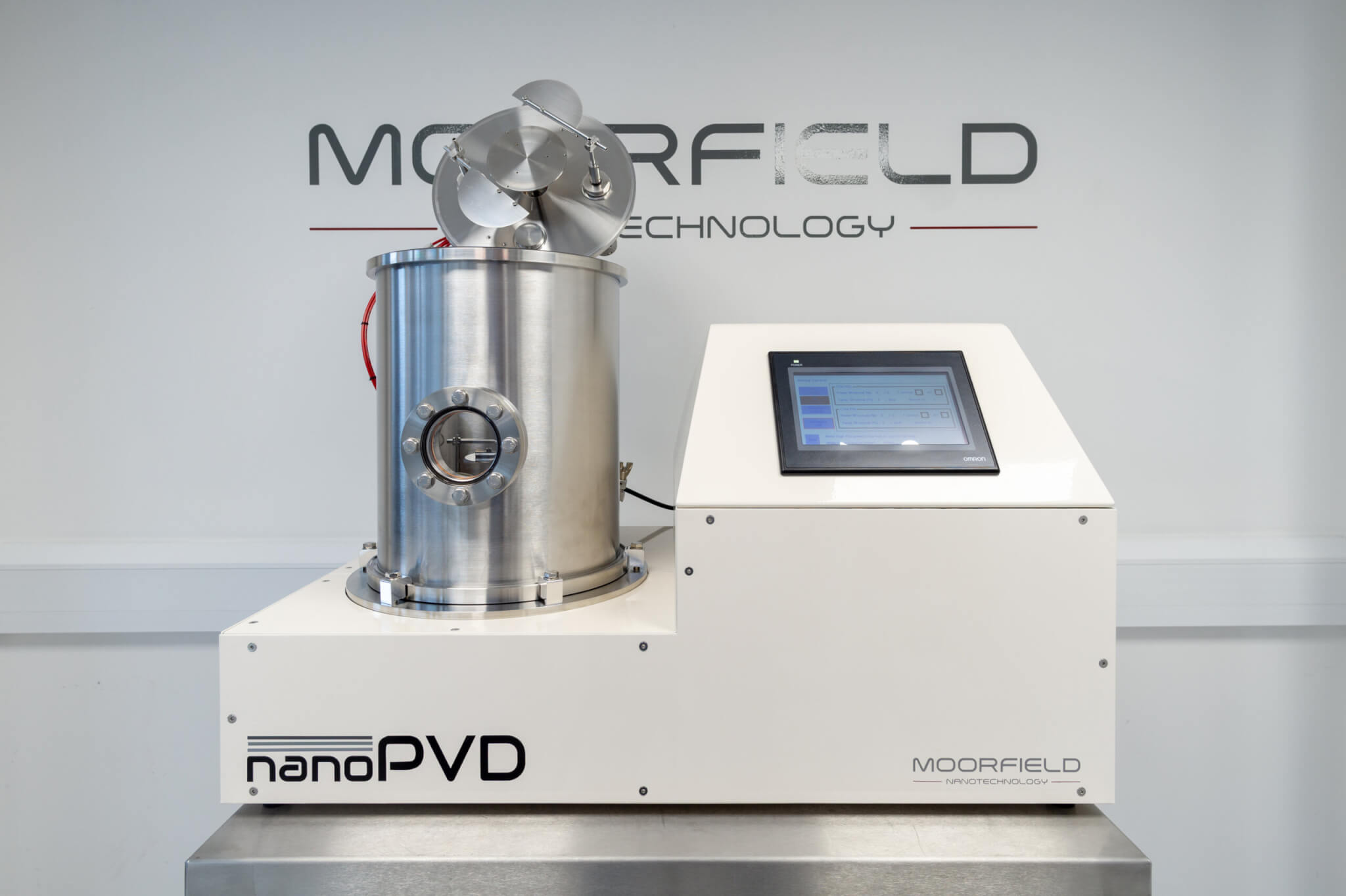
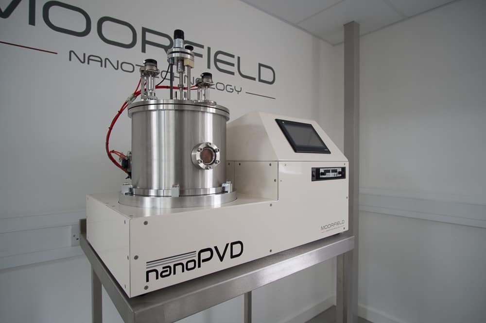
Benchtop Evaporation System
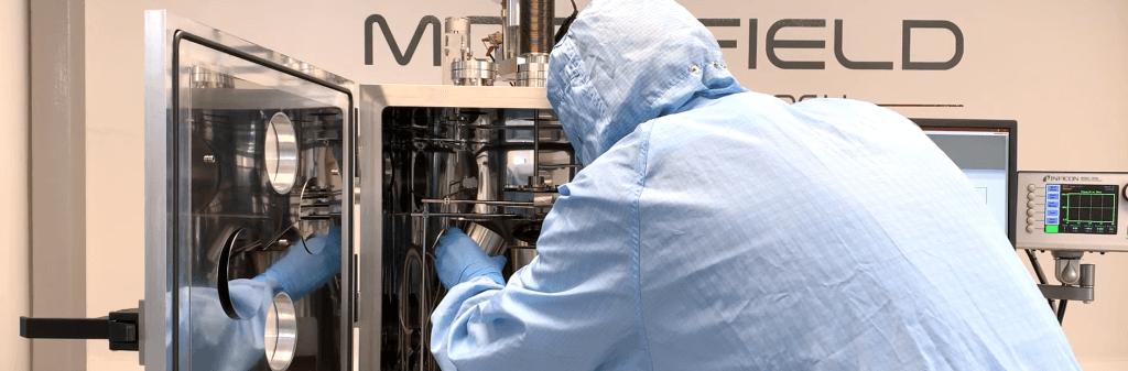
nanoPVD-T15A Thermal Evaporation System
Compact thermal and low-temperature evaporation for metals, organics and sensitive thin-film materials.
The nanoPVD-T15A gives research teams local evaporation capability where controllable thermal and low-temperature workflows matter more than sputtering source count.

Product gallery
nanoPVD-T15A image carousel

Research-grade capability without enterprise complexity
This platform is positioned for research teams that need controllable thin-film process access, practical laboratory integration and clear configuration choices.
- Compact evaporation access for research laboratories
- Thermal and low-temperature evaporation source configurations
- Useful for metals, organics, electrodes and optical films
- Recipe-led operation for repeatable development runs
- Lower infrastructure burden than larger modular systems
Benefits that matter in a working research lab
Faster evaporation cycles
Keep thermal evaporation of electrodes, contact layers and specialist materials close to the research group so early-stage process changes can happen quickly.
Ease of use for mixed-experience teams
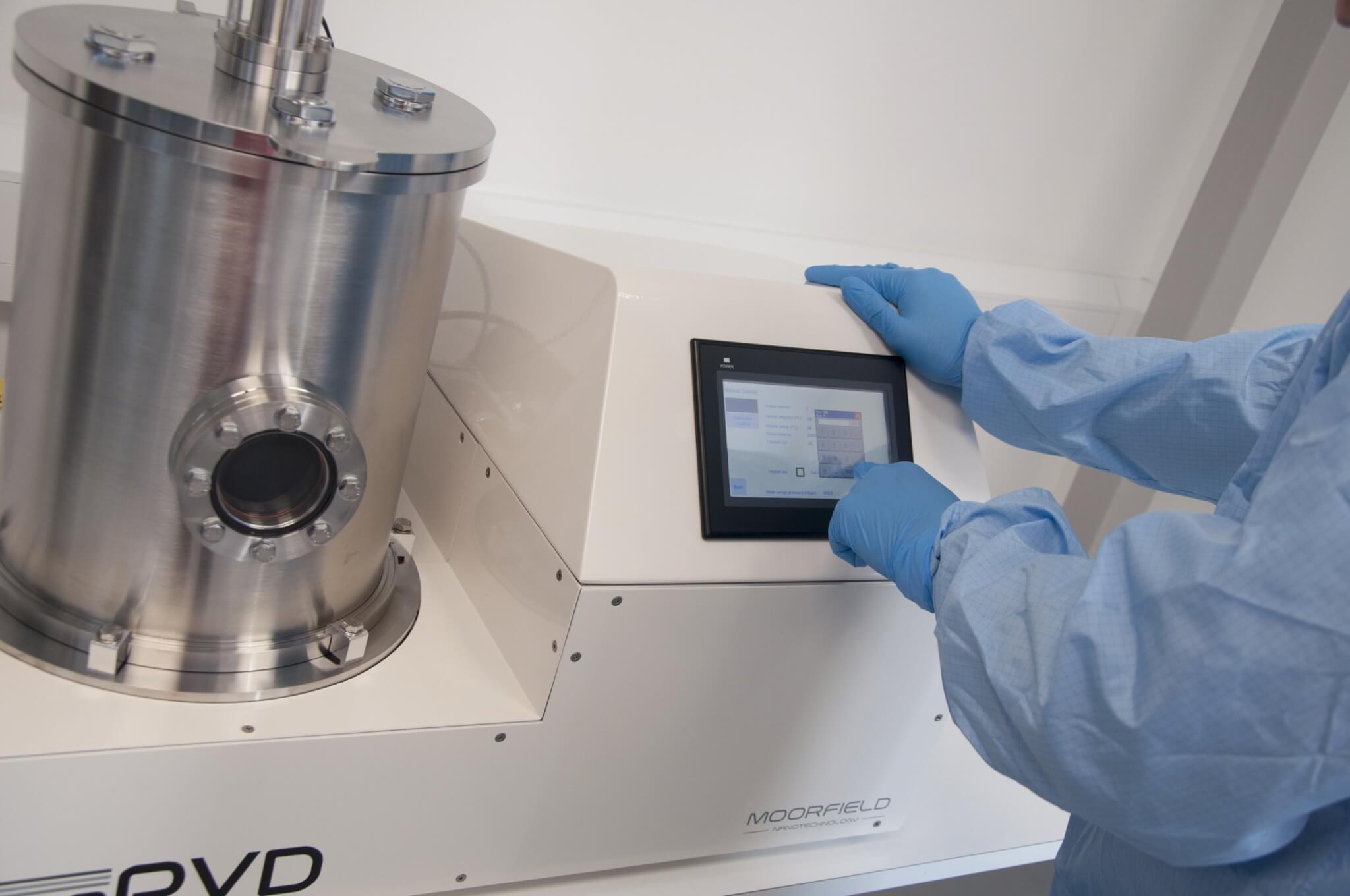
A compact format, touchscreen HMI and recipe-based operation make the platform approachable for shared labs while preserving research-grade control.
Research-grade evaporation flexibility
Supports practical evaporation methods for metals, volatile organics and sensitive materials where local access and careful process development matter.
Lower operational friction
The benchtop format gives departments useful PVD capability without the access complexity, services load and training burden of larger infrastructure.
Better use of premium tools
Develop baseline evaporation recipes locally and reserve larger shared systems for mature processes, integrated runs or higher-capacity work.
Designed for real devices
Useful for electrodes, interfaces, organic electronics, quantum-device studies, small-batch coating work and proof-of-concept materials research.
Typical configurations
Use these examples as starting points. Moorfield can refine the final specification around your materials, substrates, gases, recipes and workflow constraints.
Metals and electrodes
For research teams depositing contact metals, electrodes and interfaces.
- Thermal evaporation method
- Compact local process access
- Useful for device prototyping
Low-temperature evaporation
For volatile organics and sensitive materials that benefit from lower-temperature source configurations.
- LTE source options
- Sensitive material fit
- Organic electronics and interface research
Optical and functional films
For exploratory coating work where deposition simplicity and clean workflow matter.
- High-vacuum benchtop chamber
- Recipe-led operation
- Functional thin-film R&D
Not sure which configuration is right for your research?
Discuss Your ApplicationKey features
Compact laboratory footprint
Research-grade thin-film capability in a practical benchtop format.
Configurable process approaches
Build around sputtering, evaporation or hybrid workflows depending on the model.
Recipe-led control
Touchscreen HMI and recipe workflows improve day-to-day repeatability.
High-vacuum platform
Turbomolecular pumping supports clean, controlled deposition conditions.
Flexible gas and source options
Process gases, source count and monitoring options can be matched to the application.
Research-first support
Moorfield helps specify the platform around your materials and target films.
Options and upgrades
Configure the platform around the process approach, substrate handling, automation and laboratory services your application needs. Options are confirmed with quotation for the final build.
Technical specifications
Exact specifications depend on final configuration and should be confirmed with quotation.
| System type | Benchtop PVD / thermal and LTE evaporation |
|---|---|
| Base pressure | 5×10⁻⁷ mbar |
| Evaporation sources | Up to 4 LTE low-temperature evaporation sources |
| Thermal evaporation | TE1 + LTE sources |
| Maximum substrate size | 4" (100 mm) |
| Substrate heating | Up to 500°C optional |
| Glovebox compatible | No |
| Warranty | 2 years |
Applications
Published application-library examples and Bioz lookup results showing nanoPVD-T15A evaporation used for electrodes, organic and molecular films, sensors, energy devices and nanoscale spectroscopy workflows.
Enhanced photocurrent Quantum Dot Emission
Publication Title: Enhanced Photocurrent and Electrically Pumped Quantum Dot Emission from Single Plasmonic Nanoantennas
Lead facility: University of Cambridge
Moorfield product cited: nanoPVD-T15A
Read applicationQuantum Sensing of Copper-Phthalocyanine Electron Spins
Publication Title: Quantum Sensing of Copper-Phthalocyanine Electron Spins via NV Relaxometry
Lead facility: Not stated in publication metadata
Moorfield product cited: nanoPVD-T15A
Read applicationHigh-sensitivity ethanol vapor detection
Publication Title: High-sensitivity ethanol vapor detection using In 2 O 3 @ZnO core–shell nanomeshes fabricated via block copolymer templating
Lead facility: Warsaw University of Technology
Moorfield product cited: nanoPVD-T15A
Read applicationRechargeable Zn Microbatteries for On-Chip Use
Publication Title: A Photolithographable Electrolyte for Deeply Rechargeable Zn Microbatteries in On-Chip Devices
Lead facility: Chemnitz University of Technology
Moorfield product cited: nanoPVD-T15A
Read applicationSingle-molecule mid-infrared spectroscopy and detection
Publication Title: Single-molecule mid-infrared spectroscopy and detection through vibrationally assisted luminescence
Lead facility: University of Cambridge
Moorfield product cited: nanoPVD-T15A
Read applicationBenign Solution-Processed Sb2Se3 Nanowires
Publication Title: Benign Solution-Processed Sb2se3 Nanowires for Photovoltaic Applications
Lead facility: Ben-Gurion University of the Negev
Moorfield product cited: nanoPVD-T15A
Read applicationDecoupled High-Mobility Graphene
Publication Title: Decoupled High‐Mobility Graphene on Cu(111)/Sapphire via Chemical Vapor Deposition
Lead facility: Italian Institute of Technology
Moorfield product cited: nanoPVD-T15A
Read applicationBioz citation lookup
Publication Title: Bioz citation results for nanoPVD-T15A
Lead facility: Multiple published sources where available in Bioz
Moorfield product cited: nanoPVD-T15A
View Bioz citationsResources and next steps
Related systems


Product FAQ
Frequently asked questions
What materials can be deposited using the nanoPVD-T15A?
The nanoPVD-T15A supports thermal evaporation of metals, organics, and sensitive or low-melting-point materials that are not suited to sputtering.
Is substrate heating available on the nanoPVD-T15A?
Substrate heating options are available. Contact Moorfield to confirm temperature range and configuration for your specific application.
Can the nanoPVD-T15A be used for organic semiconductor deposition?
Yes. The low-temperature thermal evaporation approach makes it suitable for organic materials where sputtering plasma would damage the film or substrate.
Build the right nanoPVD-T15A configuration for your research
Tell us about your materials, substrates, process gases and target films. Moorfield will help specify a practical system configuration.
nanoPVD-T15A
The nanoPVD-T15A is a benchtop evaporation system optimised for deposition of various high-melting point metals and volatile organics. As compact as an electron microscopy coater, but with high-end hardware for research-grade results.
nanoPVD-T15A Benchtop PVD System
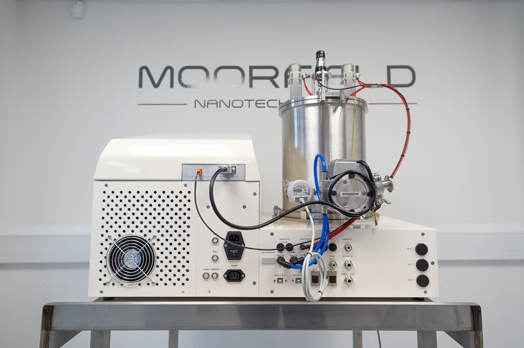
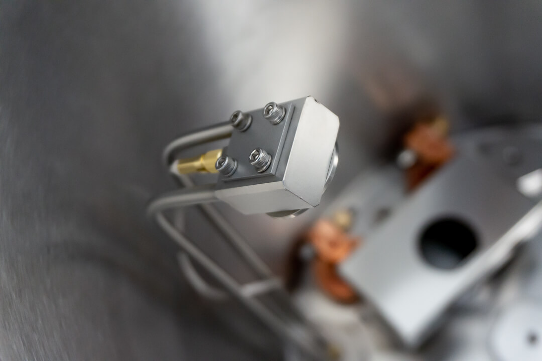
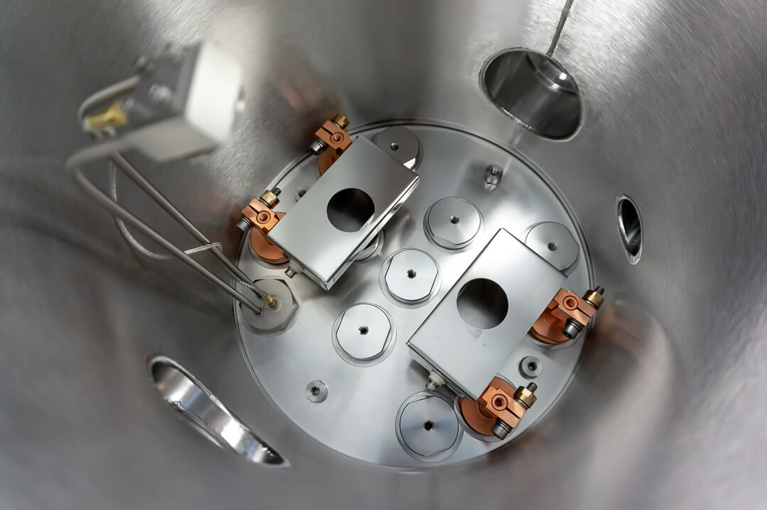
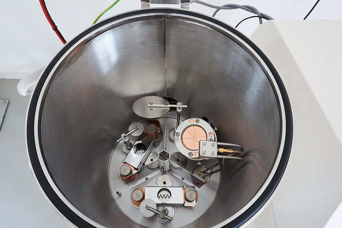
Optimised for thermal evaporation onto substrates up to 4″ diameter. It can be equipped with standard resistive evaporation sources and/or low-temperature evaporation (LTE) sources for deposition of metals and organics, respectively.
LTE sources are low thermal-mass for better control when evaporating volatile organic materials, while metals sources are our box-shielded TE1 models for efficient deposition and reduced cross-contamination.
Chamber access is via a hinged lid that opens to reveal a stage suitable for holding substrates up to 4″ in diameter. The chamber is tall, allowing for high-uniformity coating via evaporative techniques.
The units are easy to control via a touchscreen HMI interface, simple to maintain, have low running costs and come with a comprehensive range of safety features.
With a turbomolecular pumping system, high-vacuum base pressures, straightforward automated control via a touchscreen HMI and a range of options for flexible configuration, the nanoPVD-T15A is a versatile, efficient solution for world-class R&D applications.
Key features
- Benchtop configuration
- Organics and metals evaporation sources
- High aspect-ratio chamber for uniform coating
- Fully automatic operation via touchscreen HMI
- Define/save multiple process recipes
- Up to 4” diameter substrates
- Base pressures <5 × 10⁻⁷ mbar
- Equipped for easy servicing
- Comprehensive safety features
- Proven performance
Example Publications
 Powered by Bioz
Options
- Dry backing pump
- Fast chamber vent
- Up to 4 LTE sources for organics
- Up to 2 evaporation sources for metals
- 500 °C substrate heating stage
- Substrate rotation, Z-shift and shutters
- Quartz crystal sensor head


Typical configurations
Metals deposition:
Two thermal evaporation sources for metals evaporation with shutters and quartz crystal sensor head for rate/thickness calibration.
Organics deposition:
Four LTE sources for organics deposition with shutters and quartz crystal sensor head for rate/thickness calibration.
Metals and organics deposition:
Two thermal evaporation sources and two LTE sources for metals and organics PVD, with shutters and quartz crystal sensor head.
Service requirements
All nanoPVD-T15A systems require chilled water, dry compressed air, nitrogen for venting (optional), and electrical power. Exact requirements will be provided with quotations or on request.
Protect your investment and maximise uptime
 Your Moorfield system is a long-term asset that needs to operate reliably and repeatably. A Service Plan is designed to protect your investment by reducing unplanned downtime, improving system reliability, and giving your team faster access to expert support when you need it.
All plans include an annual preventive maintenance visit (with documented checks) plus remote technical support—helpful for troubleshooting issues quickly without waiting for an on-site visit. As your needs increase, higher tiers add greater consumables/parts cover, discounted call-outs and travel, priority scheduling, and training refresher days to help new users get up to speed and reduce avoidable errors.
Service Plans also support easier budgeting (fixed annual or monthly options on eligible tiers) and provide multi-system discounts.
Ask us which plan best fits your throughput demands and budget priorities using our CONTACT US FORM