

Thin-film deposition, plasma etch and anneal workflows for quantum device R&D
Compact PVD and plasma process tools for research groups developing quantum materials, metal contacts, molecular spin films, photonic structures, 2D materials and exploratory device stacks.
Moorfield systems are not presented as complete quantum-device fabrication lines. They provide configurable thin-film deposition, plasma processing and thermal process capability for selected research workflows where local, flexible process access is valuable.
Application fit
Why local process access matters in quantum-device R&D
Develop contact and interface recipes before using shared cleanroom time
Screen contact metals, adhesion layers, surface preparation steps and early device-stack options locally before transferring mature recipes to larger shared infrastructure.
Handle sensitive materials and hybrid stacks with less process disruption
Configure evaporation, sputtering, glovebox-compatible transfer or plasma preparation around organic, molecular, 2D or air-sensitive materials rather than relying entirely on general-purpose shared tools.
Support small-batch quantum materials research
Use compact and modular platforms for small substrates, shadow-mask trials, exploratory films and iterative device learning where flexibility matters more than production throughput.
Build evidence for grants, facilities access and scale-up decisions
Generate early process data, samples and device-relevant test structures before committing to high-cost cleanroom runs, external foundry work or a larger system purchase.
Published evidence
Published Moorfield-linked examples
Published examples show Moorfield systems being used in quantum sensing, quantum-dot optoelectronic and nanoscale sensing workflows. These examples are evidence of relevant process steps, not a claim that one platform covers every quantum-device fabrication workflow.
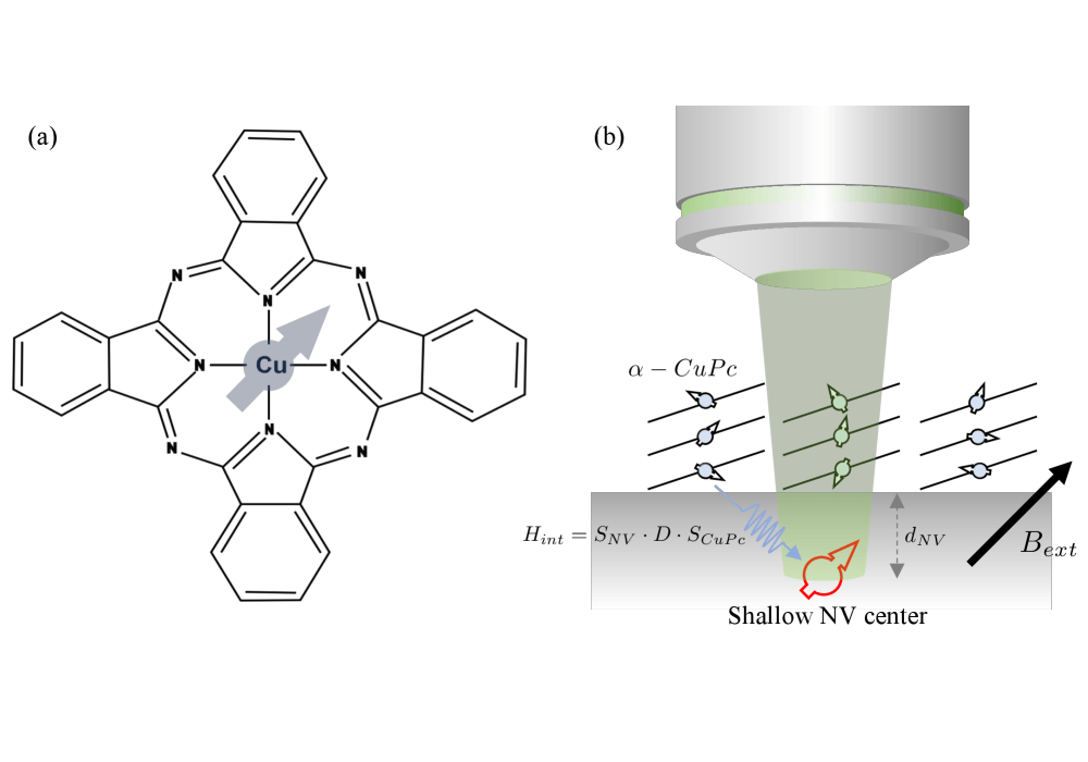
Quantum sensing of copper-phthalocyanine electron spins
A published NV-relaxometry study used copper-phthalocyanine thin films as molecular spin systems. Moorfield’s application page states that the CuPc film was thermally evaporated from powder using a nanoPVD-T15A under approximately 1 x 10^-6 Torr.
nanoPVD-T15A – thermal evaporation of CuPcElectrically pumped quantum-dot emission from plasmonic nanoantennas
The referenced ACS Nano work used Cr/Au electrode deposition by thermal evaporation with a NanoPVD-T15A, supporting a credible claim around contact metallisation for quantum-dot optoelectronic structures.
nanoPVD-T15A – Cr/Au thermal evaporationSingle-molecule detection and super-resolution imaging
This is an adjacent nanoscale sensing example rather than a primary quantum-device proof point. Moorfield’s application page states that a MiniLab 080 was used to sputter 12 nm chromium grids during sample preparation.
MiniLab 080 – chromium sputteringPossible platform fit
Relevant Moorfield platforms
The right fit depends on the process approach, material sensitivity, substrate size, source type and level of local recipe control required.
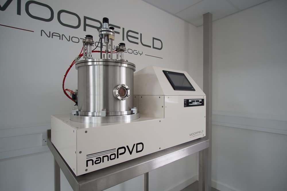
nanoPVD-S10A
Compact RF/DC magnetron sputtering for contact metals, conductive layers, oxides, nitrides and exploratory multilayer stacks used in device and materials R&D.
- Up to 3 water-cooled magnetron sources
- RF/DC sputtering for conductive and non-conductive materials
- Reactive sputtering methods for oxides and nitrides
- Useful for local recipe screening before larger cleanroom runs

nanoPVD-T15A
Thermal evaporation platform for small-batch materials research, contact metallisation and molecular thin-film deposition where the process and material are compatible.
- Published Moorfield-linked examples include CuPc evaporation and Cr/Au electrode deposition
- Suitable for shadow-mask and exploratory metallisation workflows
- Relevant where thermal evaporation is the right approach for the material

MiniLab 090
Glovebox-compatible modular PVD for air-sensitive device research, protected process transfer and advanced materials workflows.
- Glovebox-compatible approach for atmosphere-sensitive workflows
- Sputtering and evaporation methods by configuration
- Up to 11 inch substrate positioning
- Suitable where modularity and protected transfer are required

nanoETCH
Compact plasma etching and surface modification for low-power etch, surface activation and research-scale device-fabrication workflows.
- Soft-etch capability for sensitive materials where configured
- Graphene, 2D materials and semiconductor etch R&D relevance
- Fluorine RIE capability where configured
- Useful for local plasma recipe development before shared cleanroom transfer
Specification support
What Moorfield can help you specify
Not every quantum workflow needs the same tool. Moorfield can help define a practical process approach around your materials, substrate size, source type, chamber access, glovebox requirement, plasma chemistry and recipe-control needs.
Discuss your quantum materials workflow
Share your material system, substrate size, process approach, environmental sensitivity and target film stack. Moorfield can help identify whether a benchtop, modular or glovebox-compatible configuration is the right fit.