Real-world applications of Moorfield products in science
Inkjet-Printed 3D Sensor Arrays

Inkjet-Printed 3D Sensor Arrays with FIB-Induced Electrode Refinement for Low-Noise Amperometric Recordings in hiPSC-Derived Brain Organoids
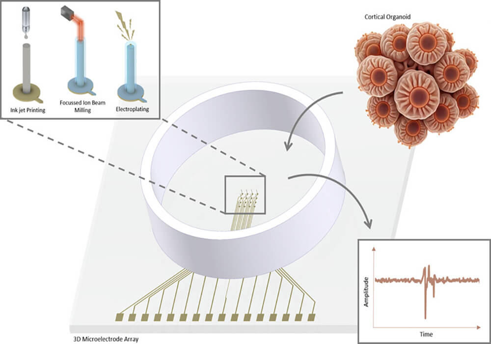
Understanding the functional connectivity and behavior of 3D cell cultures and organoids requires monitoring electrical activity across multiple planes. However, traditional planar microelectrode arrays (MEAs) are limited to surface recordings and struggle to capture signals from deeper layers. Additionally, current fabrication methods face challenges such as prolonged production times and limited design flexibility, which hinder the development of high-precision 3D electrode arrays and affect the quality of cell-electrode coupling. To overcome these obstacles, we introduce a new approach that integrates inkjet printing with focused ion beam (FIB) milling and electrodeposition, resulting in highly customizable 3D MEAs. The FIB milling enables the creation of precise electrode openings at predetermined locations, which is essential for selective recordings within the tissue. The MEAs, fabricated on glass substrates, incorporate high-aspect-ratio (up to 44:1) electrode structures with heights up to 1 mm, a pitch of 500 μm, and electrode openings of 3 and 6 μm, providing the necessary resolution for targeted measurements. Impedance and noise characteristics (down to a root-mean-square of (RMS) noise of 0.2 pA) for amperometric measurements were assessed in dependence on the electrode size. We demonstrate the effectiveness of these 3D MEAs by recording electrophysiological activity from hiPSC-derived cortical organoids (age: 24 month) both in situ and after 10 days of cultivation of the organoid directly on the MEA. This approach facilitates in vitro studies of neural activity in organoids and holds promise for high-throughput, selective amperometric analyses in normal and pathologically altered conditions.
How Moorfield products helped:
nanoPVD
Electrode Fabrication
Reagents were purchased from Sigma-Aldrich, USA, unless otherwise specified. 3-in. glass wafers (Borosilicate glass 3-in. glass wafer, MicroChemicals GmbH, Ulm, Germany; thickness: 500 μm) were cleaned using an ultrasonication bath (Bransonic ultrasonic cleaner 5510E-MTH, Branson ultrasonics, USA) for 5 min in acetone (VLSI Selectipur, BASF SE, Germany), 2-Propanol (99.5%) (IPA), and deionized (DI) water (Ultra Clear purification system/Berry Tec, Germany), respectively. Each 3-in. substrate yielded four MEAs. Lithography and lift-off procedures were employed to generate the electrode area, contact traces, and connection pads. A 50 nm thick layer of photoresist (Ma-N 1410, micro resist technology, Berlin, Germany) was spin-coated (Polo Spin 150i, Netherlands; 500 rpm for 10 s, followed by 3000 rpm for 25 s) on top of the cleaned substrate, exposed using a maskless aligner system (μMLA, Heidelberg Instruments Mikrotechnik GmbH, Heidelberg, Germany; dose: 160 mJ·cm–2, defoc: 0), kept for 3 min in developer (ma-D 533/s, micro resist technology, Berlin, Germany), rinsed with DI water, and dried in air. Afterward, a layer stack of 15 nm Ti and 100 nm of Au (5 × 10³ mbar argon, 12 W Au, 40 W Ti, Moorfield nanoPVD, UK) was sputtered on the glass slides.
Open Access publication details:
Inola Kopic, Hu Peng, Sebastian Schmidt, Oleksandr Berezin, Senyao Wang, Gil G. Westmeyer, and Bernhard Wolfrum ACS Sensors 2025 10 (9), 6426-6435 https://pubs.acs.org/doi/10.1021/acssensors.4c03740
